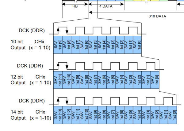
【DAQ Systems】高速ADC的HDL设计(二)一个基于AXI-Stream总线的高速ADC IP核代码解析 Tags: FPGA, Verilog, 通信, 项目 Post author:TerayTech Post published:2022年6月11日 Post category:EDA / 嵌入式 / 所有文章 / 硬件 Post comments:0评论 Post last modified:2022年8月14日 Reading time:1 mins read 写文章太累,本篇采用视频的形式~ 打印 🖨 .PDF 📄 电子书 📱 打赏赞(2)微海报分享 Read more articles Previous PostW800上手 Part.1 点个RGB 在下一篇文章W800上手 Part.2 AOS开发入门 发表回复 取消回复CommentEnter your name or username to comment Enter your email address to comment Enter your website URL (optional) 在此浏览器中保存我的显示名称、邮箱地址和网站地址,以便下次评论时使用。 Δ 你可能也喜欢 FPGA实现索尼传感器subLVDS接口接收(以IMX178为例) 2025年1月31日 EVMeter-石剑篇 2020年5月21日 做一个锁定放大器! 2021年8月13日 把闲置的树莓派变成一个桌面监视器 2021年6月30日 微观尽头——精密信号测量:Intro 2021年9月23日